Things to Keep in Mind When Designing a 4 Layer PCB
Printed circuit boards have come a long way; from single layered PCBs to 4 layered PCBs, while some going up to 32 layers. Integrated circuits, microprocessors, and microcontrollers are getting smaller and powerful each day and this has resulted in the fabrication of PCBs with more than one layer. Nowadays,
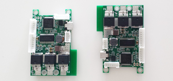
2 layered PCB fabrication is quite common and is mostly carried out by electronic hobbyists and small industries.
There are certain factors that need to be kept in mind before you design a 4 layered PCB. This is known as a design plan and it is basically a brief understanding on the routing methods involved, what needs to be routed in the beginning, and the presence of any high speed signals.
Identification of the Different Layers
Before you begin designing a 4 layered board, you have to determine the function of each layer. This is called a ‘PCB stack-up’. You can consider things like which layer is for the power (VCC), which layer is for the ground, and which layer might be used for an analog or a digital signal. For example in a 6 layered PCB, it will be as follows:
- First layer: Normal traces
- Second layer: The 5 V power plane (VCC)
- Third and Fourth layer: FLASH and RAM high speed routing
- Fifth layer: The ground plane (0 V)
- Sixth layer: Normal traces
Analog and Digital Lines
As an electronic hobbyist, you should be aware of the differences between an analog signal and a digital signal. This is important while designing a 4 layer PCB. Suppose you are designing a PCB which will consist of a FPGA or a microcontroller along with an ADC (analog to digital converter). If the ADC is of 16 bits, you have to isolate the digital and analog planes within the PCB.
You can do this by utilizing a layer between the analog and digital planes as a ground plane, or you can also use an entire layer for routing an analog or a digital signal. This will enable your PCB to stand out from one with a lot of noise.
Separating the High Speed Line
If you are fabricating a 4 layer PCB with a high speed signal component like a USB, external RAM, or a fast ADC or DAC, it is vital that you separate out the high speed line. Let’s say that you are generating a frequency of 100 MHz; at this frequency, the trace layer will act like an antenna, a capacitor, a resistor, and a coil simultaneously. This can cause an inconsistency in the timing signal of a RAM circuit and can cause crosstalk in communication circuit boards.
You can prevent this by locating the high speed signal next to a ground plane or dedicating an entire layer for high speed signal routing with two ground planes underneath and above it. This is mostly done for signals with a frequency of more than 500 MHz.