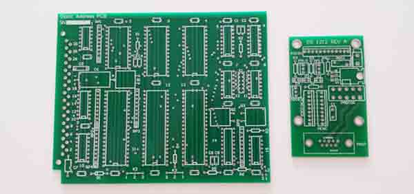
Understanding 2-layer PCB and its Fabrication
Today, majority of the printed circuit boards being produced feature an odd number of layers (greater than 1). The 2-layer PCB automatically falls in this category, but the journey from single-sided PCB’s to 2-layer PCBs is fraught with challenges. The rewards on offer make the effort worth it though.
Without point-to-point soldering, 2- layer PCB increase density and allows traces to cross over each other. The fabrication process of double-sided printed circuit boards is pretty much the same as the
fabrication process of single-sided PCB’s. However, there is one major difference—you have to etch both sides and transfer artwork.
The hardest part in the fabrication of double-sided
quality PCB is correctly aligning both sides and transferring the artwork. Furthermore, you must ensure that both sides stay properly aligned during UV exposure. The reason for this is simple—the hole will be in the center on the bottom side of the equivalent pad when you drill holes through a pad on the top half if both sides are correctly aligned. The most common reason manufacturers are unable to produce
quality PCB is inappropriate artwork alignment. Finally, when designing a double-sided board you must follow specific rules before etching your board. Following are the specific guidelines that you need to keep in mind when making 2-sided printed circuit boards.
Aligning both sides
Getting both layers to align with each other is the hardest part of making two-layer circuit. You won’t be able to pass alignment pins through the set of hold if both sides aren’t appropriately aligned. Ideally, you shouldn’t be off by more than one-tenth of an inch.
Clean transfer
At times, some of the resist fails to transfer to the copper after you’ve drilled the alignment holes and ironed the film. Most of the times dust from the drilled alignment holes causes this. Therefore, once you’re done drilling you must clean the board.
Prepare your board for exposure to UV light
It is important that you prepare both sides of your board for exposure to UV light only when your artwork is good to go. Once you have good quality artwork, make sure that both sides of your board are exposed to Ultraviolet light. Furthermore, you can develop and etch the board.
Test accuracy
In order to test the accuracy of the board, make a few stochastic component holes throughout the board using a drill machine once you’ve developed and etched the printed circuit board.
Inspect
It is important that you inspect your board once you’ve developed and etched it. Your alignment is excellent if the translucent board shows both layers when you hold it up with a light behind it after etching. Furthermore, traces end and pass through to the appropriate trace on the other side.
Making single-sided boards is easy enough. Unfortunately, the same cannot be said about double-sided boards. However, by following the guidelines mentioned above, you can make a quality PCB or printed circuit board.